Prime Minister Narendra Modi’s visit to Singapore is crucial for India’s semiconductor ambitions. During his trip, India and Singapore signed agreements to enhance collaboration on semiconductor cluster development and talent cultivation in the sector. Singapore, with a well-established semiconductor industry, contributes 10% of global semiconductor output and 5% of wafer fabrication capacity. This partnership strengthens India’s semiconductor ecosystem, which has seen a significant boost since launching the India Semiconductor Mission in 2021. India’s abundant land and labour offer opportunities for Singapore’s semiconductor companies to expand while benefiting from Singapore’s expertise and infrastructure.
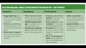
India’s semiconductor market is growing rapidly, with the electronics market expected to reach US$300 billion by 2026-27. Semiconductor consumption is projected to reach US$75 billion by 2027, and India is poised to capture a significant share of the global market, which is expected to grow to US$1 trillion by 2030.

The evolution and importance of semiconductors
In 1874, Karl Braun discovered and documented the first semiconductor diode effect. He observed that current flows freely in only one direction at the contact point between a metal and a galena crystal. In 1901, the first semiconductor device, known as “cat whiskers,” was patented.
Semiconductors: Brains of modern electronics
Semiconductors are essential components of modern electronics, enabling advancements in fields like communication, computing, healthcare, military systems, transportation, and clean energy. A semiconductor’s electrical resistance is higher than a conductor’s but lower than an insulator’s, allowing it to conduct current at a controlled rate—neither too fast nor fully restricted.
These materials are crucial for producing cell phones, satellite systems, and other communication devices. Semiconductors also enable wireless communication, network equipment, and hardware for data transmission. Beyond consumer electronics, semiconductors power essential social infrastructure, such as bank ATMs, trains, the internet, and medical networks used for elderly care.
Unlike vacuum tubes, semiconductors are shock-resistant, smaller, more compact, and consume less power. While semiconductors are sensitive to temperature and radiation, they are cheaper and longer-lasting than vacuum diodes. They exhibit a variety of useful properties, including variable resistance, unidirectional current flow, and sensitivity to light and heat. Their key functions include signal amplification, switching, and energy conversion.
Types of semiconductors
n-type semiconductors: These are intrinsic semiconductors doped with elements like phosphorus (P), arsenic (As), or antimony (Sb). In n-type semiconductors, electrons serve as charge carriers, making them more efficient than p-type semiconductors, where holes act as charge carriers.
p-type Semiconductors: These are doped with elements that create holes (positive charge carriers), but n-type semiconductors are generally more effective due to the higher mobility of electrons.
Materials and advancements in semiconductor technology
Silicon: Silicon, with 14 electrons, forms a single crystal when it crystallizes, making it an ideal material for semiconductor products. The electrical properties of silicon can be altered through doping. As one of the most abundant elements in the Earth’s crust, silicon is the cheapest material for semiconductor applications, making it the most widely used.
Diamond: Diamond is a semiconductor with an ultra-wide bandgap and the highest thermal conductivity, allowing it to transfer heat efficiently, surpassing traditional materials like silicon.
Advanced semiconductor technologies: IBM’s 2-nanometer chip technology integrates 50 billion transistors, each the size of about five atoms, onto a space no larger than a fingernail, pushing the boundaries of semiconductor capabilities.
Also read India’s GDP Growth Slows To 6.7% In Q1 2024 Amid Agriculture Decline
India’s latest steps for semiconductor push
According to a PIB report on September 2, 2024, the Union Cabinet, chaired by Prime Minister Narendra Modi, approved Kaynes Semicon Pvt Ltd’s proposal to set up a semiconductor unit in Sanand, Gujarat under the India Semiconductor Mission (ISM). The unit will be established with an investment of Rs 3,300 crore and will have the capacity to produce 60 lakh chips per day. The chips produced will serve various sectors, including industrial, automotive, electric vehicles, consumer electronics, telecom, and mobile phones.
In June 2023, the Union Cabinet approved the first semiconductor unit in Sanand, Gujarat. In February 2024, three additional semiconductor units were approved.
Also read: First silicon carbide manufacturing facility to be set up in Odisha
Policy initiatives:
Make in India: This initiative aims to transform India into a global hub for Electronic System Design and Manufacturing (ESDM).
PLI Scheme: In December 2021, the Centre sanctioned Rs 76,000 crore under the production-linked incentive (PLI) scheme to encourage the manufacturing of various semiconductor goods within India.
DLI Scheme: It offers financial incentives and design infrastructure support across various stages of development and deployment of semiconductor designs for Integrated Circuits (ICs), Chipsets, Systems on Chips (SoCs), Systems & IP Cores, and semiconductor-linked design.
Digital RISC-V (DIR-V) Program: This program intends to enable the production of microprocessors in India, aiming to achieve industry-grade silicon and design wins by December 2023.
India Semiconductor Mission (ISM): The mission aims to build a vibrant semiconductor and display design and innovation ecosystem, enabling India’s emergence as a global hub for electronics manufacturing and design.
Launched in 2021 with a financial outlay of Rs 76,000 crore under the Ministry of Electronics and IT (MeitY), ISM is part of a comprehensive program for developing sustainable semiconductor and display ecosystems. It provides financial support to companies investing in semiconductor and display manufacturing and design. Led by global experts in the semiconductor and display industry, ISM will serve as the nodal agency for efficient and coherent implementation of the schemes.
MoU with European Commission: In 2023, the Union Cabinet was informed about a Memorandum of Understanding (MoU) signed between the Government of India and the European Commission on working arrangements for the semiconductor ecosystem, its supply chain, and innovation under the framework of the EU-India Trade and Technology Council (TTC).
Also read: Singapore Business Leader Aims to Double India Investments After PM Modi’s Roundtable
The government plans to increase the funding outlay for the second phase of its chip manufacturing incentive policy to $15 billion, up from the $10 billion committed in the first phase.
Actionable steps for growth:
1. Focus on analog, power, and discrete semiconductors instead of advanced digital tech.
2. Target 45nm and 28nm technologies for long-term engagement.
3. Expand talent and successful models like SFAL to other cities.
4. Attract global Indian talent with competitive offers.
Investments required for the semiconductor industry
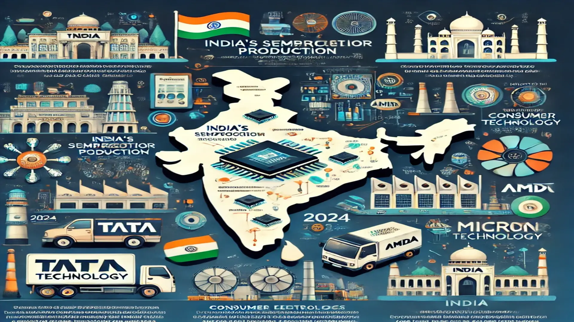
India is actively seeking foreign investments to develop its indigenous semiconductor industry, focusing on fabs, ATMPs (Assembly, Testing, Marking, and Packaging), and other critical infrastructure. Recent developments signal India’s ambition to create a strong semiconductor ecosystem by 2030.
Recent developments: As of September 5, 2024, India and Singapore signed multiple agreements during Prime Minister Narendra Modi’s visit, including collaborations on semiconductor cluster development and talent cultivation for semiconductor design and manufacturing. The Indian government announced that the construction of four approved semiconductor units is progressing rapidly. These units are expected to attract INR 1.5 trillion (US$18.15 billion) in investments and will have a combined production capacity of around 70 million chips per day. The projects include a Tata-PSMC commercial fab plant and three ATMP/OSAT plants.
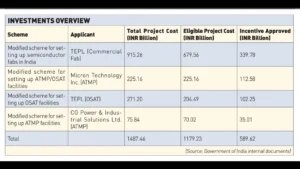
In addition, the Kaynes Semicon unit in Sanand, Gujarat, will produce six million chips per day across various industries such as automotive, consumer electronics, telecom, and mobile phones. The Union Cabinet approved Kaynes Semicon’s Rs 33.07 billion (US$394.15 million) investment for this project, making it the fifth semiconductor unit approved under the India Semiconductor Mission.
Key projects and initiatives:
Assam’s Semiconductor Facility: The Assam government has signed a 60-year lease agreement with the Tata Group to establish a semiconductor unit in Morigaon, investing Rs 270 billion. The first chip is expected to be produced by 2025.
AMD partnership: In July 2024, AMD partnered with IIT Bombay to fund startups developing energy-efficient Spiking Neural Network (SNN) chips, supporting India’s innovation in semiconductor design.
Local startups: Several Indian semiconductor startups, including Saankhya Labs and Netrasemi, are contributing to building a robust semiconductor ecosystem.
Key International Collaborations:
Tata-PSMC Fab Plant: Tata Electronics, in collaboration with Powerchip Semiconductor Manufacturing Corporation (PSMC), plans to establish a semiconductor fabrication facility in Dholera, Gujarat, with an Rs 910 billion (US$11 billion) investment, creating 20,000 skilled jobs. The fab will produce 50,000 wafers per month.
Micron Technology: Micron’s ATMP facility in Sanand, Gujarat, will begin operations by 2025, with Phase 2 expansion planned for the second half of the decade. This project is expected to create 5,000 jobs.
Future opportunities: As India strengthens its semiconductor ecosystem, there is potential for additional investments through schemes like the Product Linked Incentive (PLI) and Design Linked Incentive (DLI), targeting areas such as SOC development, ATMP facilities, and fabless ecosystems.